![]() Alaee et al. recently reported the observation of "extreme coupling" in plasmonic systems. We will describe how the experiment may give plasmonics new perspectives - both in applications and in fundamental research.
Alaee et al. recently reported the observation of "extreme coupling" in plasmonic systems. We will describe how the experiment may give plasmonics new perspectives - both in applications and in fundamental research.
Plasmonics is a field of electromagnetic research in which researchers try to exploit the interaction of light with conduction electrons of metals. This interaction leads to the advent of so-called Surface Plasmon Polaritons, quasi-particles characteristic for an ongoing energy exchange between the electromagnetic field and collective electron oscillations.
In a metallic particle, the collective electron oscillation can form standing waves just like those observable in guitar strings. Technically, this effect can be attributed to Fabry-Perot resonances rendering the metallic particle a plasmonic resonator. The main difference of plasmonic resonators compared to optical resonators based on dielectric materials like fused silica, is the possibility to focus energy to tiny spots way below the wavelength, since plasmonic resonators may be as small as a few nanometers.
However, most practical devices like solar cells or detectors usually have a flat metallic back-plate, for which the wavelength of Surface Plasmon Polaritons and thus dimensions of possible resonant structures are only slightly smaller than the wavelength. So, although plasmonic excitations of a flat surface exist, one may sacrifice the biggest advantage of plasmonic devices: the localization of energy to small volumes.
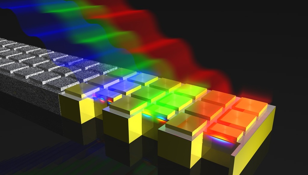
 Illustration of the device to observe extreme coupling: gold nanopatches above a gold backplate. Local electric fields at first (red wave), second (green wave) and third resonance (blue wave) visualized in cuts.
The Realization of Deep-Subwavelength Plasmonic Resonators
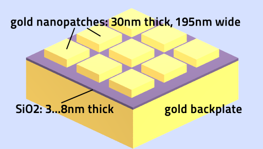
One approach to achieve an extreme energy localization involving a flat metallic backplate was just recently demonstrated by R. Alaee et al. in "Deep-Subwavelength Plasmonic Nanoresonators Exploiting Extreme Coupling" which will soon appear in Nano Letters. Using a technique called atomic layer deposition, the team of researchers managed to place thin golden nanopatches just 3nm to 8nm above a golden back plate. The nanopatches with lengths of roughly 200nm and a thickness of 30nm were all equally sized for a given realization and regularly placed to form a lattice of plasmonic resonators, see Figure on the right. Because of the tiny separation between the nanopatches and the backplate, their respective Surface Plasmon Polaritons are strongly coupled.
It is generally known that a coupling results in new modes as a combination of the modes of the respective subsystems, symmetric and antisymmetric modes appear. In the given experiment, these modes might be understood in terms of the symmetric and antisymmetric oscillations of the electrons in the nanopatches and the backplate, respectively. In this notion, the energy of the symmetric mode is generally higher than the antisymmetric one. The coupling due to the tiny separation realized by Alaee et al. is able to shift the resonance of the antisymmetric mode with respect to the isolated structures from optical frequencies to mid-infrared frequencies with less than one third of the original energy. Such a tremendous energy shift may very well justify the notion of "extreme coupling" used by the authors.

Extreme Coupling Perspectives
What is the extreme coupling good for? In the article, it is exemplarily shown, how such a structure can be used to almost fully absorb light at a certain frequency. This is realized due to the strong fields inside the gap that also penetrate the metallic parts, where the energy gets absorbed due to Ohmic losses. Nevertheless, other applications enabled by the proposed extreme coupling scheme appear much more compelling.
The main advantage of the fabricated structure is its size: The plasmonic resonators are way smaller than the wavelength. Hence, if for example a signal hits the device, processing times along the structure ought to be extremely fast. However, the losses inside the metal may prevent such applications from being highly efficient, at least at room temperature. Plasmonic detectors based on extreme coupling schemes may thus always need to be designed with respect to a suitable tradeoff between ultrafast response times and detection efficiency.
But there are other applications than ultrafast detectors that may benifit from extremely coupled plasmonic resonators. Alaee et al. point out that they used a thickness of at least 3nm to not enter regimes in which quantum effects might play a dominant role. The reason is that it is much more easy to confirm an effect with respect to classical electrodynamics than within quantum electrodynamics.
Nevertheless, questions in plasmonic research aiming for new insights with respect to quantum effects are hugely discussed at the moment; the newly arising field of quantum plasmonics attracts much attention. The setup investigated by Alaee and co-workers may help to understand the influence of quantum effects, if it will be possible to reduce the dielectric gap down to a single nanometer or even further. This seems feasible as the used technique, atomic layer deposition, is able to coat a surface with layers made of single atoms.
Whatever the route will be Alaee and co-workers will take - detector applications or fundamental quantum plasmonic research - it is clear that the observation of extreme coupling in plasmonic systems is a true cornerstone in plasmonic research and fabrication. The hunt is on to conquer the last nanometer!


