Tags: Dispersion Relation / Permittivity
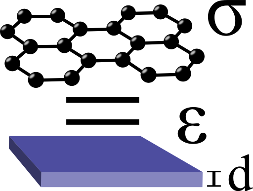
![]() Graphene is a monolayer of carbon atoms and offers extremely interesting physics. Its unique properties may very well make it the silicon of the 21st century. For practical applications it is of great importance to model this material containing the main electromagnetic features. Find out in this problem how graphene can be represented as a thin layer with a certain permittivity and how this can be used for next-generation electromagnetic devices.
Graphene is a monolayer of carbon atoms and offers extremely interesting physics. Its unique properties may very well make it the silicon of the 21st century. For practical applications it is of great importance to model this material containing the main electromagnetic features. Find out in this problem how graphene can be represented as a thin layer with a certain permittivity and how this can be used for next-generation electromagnetic devices.
Problem Statement
Find the dispersion relation of transverse magnetic surface plasmon polaritons (SPPs) supported by graphene embedded in some medium with relative permittivity \(\varepsilon_{d}\)!
You may want to follow these steps:
- Start from Ampère's law including the displacement current to figure out a relation between:
- permittivity \(\varepsilon\left(\omega\right)\) and
- a three-dimensional conductivity \(\sigma\left(\omega\right)=\sigma_{2D}\left(\omega\right)/d\)
- assuming a certain thickness \(d\) of graphene.
- Regard graphene now as a metallic layer with thickness \(d\) and relative permittivity \(\varepsilon_{m}\left(\omega\right)\)
- Use the dispersion relation of transverse magnetic SPPs to find the wave-vector in the limit of vanishing thickness \(d\).
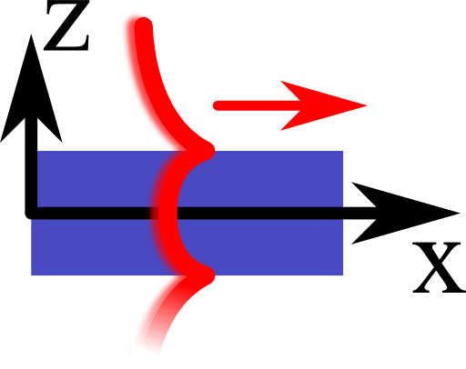
The dispersion relation for the wave vector \(k_{p}\left(\omega\right)\) of such an SPP supported by the given layer reads as
\[\begin{eqnarray*}\tanh\left\{ \sqrt{k_{p}^{2}-\varepsilon_{m}k_{0}^{2}}\frac{d}{2}\right\} & = & -\frac{\sqrt{k_{p}^{2}-\varepsilon_{m}k_{0}^{2}}\varepsilon_{d}}{\sqrt{k_{p}^{2}-\varepsilon_{d}k_{0}^{2}}\varepsilon_{m}}\ .\end{eqnarray*}\]
Hints
In frequency space, Ampère's law reads
\[\nabla\times\mathbf{B}\left(\mathbf{r},\omega\right)=\mu_{0}\mathbf{j}\left(\mathbf{r},\omega\right)-\mathrm{i}\omega\mu_{0}\varepsilon\left(\mathbf{r},\omega\right)\mathbf{E}\left(\mathbf{r},\omega\right)\ .\]
Do you know a relation between \(\mathbf{j}\) and \(\mathbf{E}\) involving \(\sigma\)?
Can you interpret the conductivity term in Ampère's law as a contribution to the permittivity?
Let us now find out the permittivity of graphene!
We have to clearify two things to find the desired dispersion relation. First we have to find a relationship between permittivity and conductivity. Second we have to calculate the vanishing thickness limit of the SPP dispersion relation using the found relative “permittivity” of graphene with respect to this thickness.
From Conductivity to Permittivity
In Ampère's law,
\[\begin{eqnarray*}\nabla\times\mathbf{B}\left(\mathbf{r},\omega\right) & = & \mu_{0}\mathbf{j}\left(\mathbf{r},\omega\right)-\mathrm{i}\omega\mu_{0}\varepsilon\left(\omega\right)\mathbf{E}\left(\mathbf{r},\omega\right)\end{eqnarray*}\]
we can use Ohm's law \(\mathbf{j}\left(\mathbf{r},\omega\right)=\sigma\left(\mathbf{r},\omega\right)\mathbf{E}\left(\mathbf{r},\omega\right)\)to find
\[\begin{eqnarray*}\nabla\times\mathbf{B}\left(\mathbf{r},\omega\right) & = & \mu_{0}\sigma\left(\mathbf{r},\omega\right)\mathbf{E}\left(\mathbf{r},\omega\right)-\mathrm{i}\omega\mu_{0}\varepsilon\left(\mathbf{r},\omega\right)\mathbf{E}\left(\mathbf{r},\omega\right)\\& = & \mu_{0}\left(\sigma\left(\mathbf{r},\omega\right)-\mathrm{i}\omega\varepsilon\left(\mathbf{r},\omega\right)\right)\mathbf{E}\left(\mathbf{r},\omega\right)\\& = & -\mathrm{i}\omega\mu_{0}\tilde{\varepsilon}\left(\mathbf{r},\omega\right)\mathbf{E}\left(\mathbf{r},\omega\right)\ .\end{eqnarray*}\]
The latter equation states that by using Ohm's law we can interprete the conductivity as a contribution to the permittivity \[\begin{eqnarray*}\tilde{\varepsilon}\left(\mathbf{r},\omega\right) & = & \varepsilon\left(\mathbf{r},\omega\right)+\mathrm{i}\frac{\sigma\left(\mathbf{r},\omega\right)}{\omega}\ .\end{eqnarray*}\]For graphene we have only given a two-dimensional conductivity and have to divide by the thickness to obtain a three-dimensional analog. We find the “permittivity” of graphene as\[\begin{eqnarray*}\tilde{\varepsilon}\left(\omega\right)=\varepsilon_{0}\varepsilon_{m}\left(\omega\right) & = & \varepsilon_{0}\left(1+\mathrm{i}\frac{\sigma_{2D}\left(\omega\right)}{\varepsilon_{0}\cdot\omega\cdot d}\right)\ .\end{eqnarray*}\]
The Vanishing Thickness Limit
A Taylor expansion of the tangens hyperbolicus for small arguments is given by \[\begin{eqnarray*}\tanh\left(x\right) & = & x-\frac{x^{3}}{3}+\mathcal{O}\left(x^{5}\right)\ .\end{eqnarray*}\]We use this approximation in the dispersion relation and obtain\[\begin{eqnarray*}\tanh\left\{ \sqrt{k_{p}^{2}-\varepsilon_{m}k_{0}^{2}}\frac{d}{2}\right\} & \approx & \sqrt{k_{p}^{2}-\varepsilon_{m}k_{0}^{2}}\frac{d}{2}\\& = & -\frac{\sqrt{k_{p}^{2}-\varepsilon_{m}k_{0}^{2}}\varepsilon_{d}}{\sqrt{k_{p}^{2}-\varepsilon_{d}k_{0}^{2}}\varepsilon_{m}}\ .\end{eqnarray*}\]In the last step we have included the relative “permittivity” of graphene. However in the limit of vanishing thickness we can neglect the one in the denominator and find\[\begin{eqnarray*}k_{p}^{2} & \approx & \varepsilon_{d}k_{0}^{2}-\left(2\frac{\varepsilon_{0}\varepsilon_{d}\cdot\omega}{\sigma_{2D}\left(\omega\right)}\right)^{2}\\& = & \varepsilon_{d}k_{0}^{2}\left[1-\varepsilon_{d}\left(2\frac{\varepsilon_{0}c}{\sigma_{2D}\left(\omega\right)}\right)^{2}\right]\\ & = & \varepsilon_{d}k_{0}^{2}\left[1-\left(\frac{2}{\eta\cdot\sigma_{2D}\left(\omega\right)}\right)^{2}\right]\end{eqnarray*}\] where we have used the free space wave vector \(k_{0}=\omega/c\) and the impedance \(\eta=\sqrt{\mu_{0}/\varepsilon_{0}\varepsilon_{d}}\) of the surrounding medium in the last two steps. See Hanson's Dyadic Green's functions and guided surface waves for a surface conductivity model of graphene for a derivation of this relation using other methods.
The found dispersion relation allows some physical interpretation. We can see that if for a given frequency the conductivity approaches high values, \(k_{p}\rightarrow\varepsilon_{d}k_{0}^{2}\), hence graphene acts as a perfect metal as expected. On the other hand, if we look at the conductivity again and set \(\Gamma=0\), \(\sigma_{2D}\left(\omega\right)\) is a purely imaginary function. So for low conductivities \(k_{p}\gg k_{0}\).
This makes it possible to build resonant graphene devices that are much smaller than the wavelength. Antennas in THz frequencies for example can be in the order of just a few hundred nanometers for wavelengths of several tens of microns.
Background: Graphene - a Material with Tunable Conductivity
The main results for the physical quantities of graphene follow from calculations which are a little too complex to be presented here. In short, the properties of the material are related to its high conductivity \(\sigma_{2D}\). Furthermore, \(\sigma_{2D}\) can be tuned using the electric field effect (EFE) applying a certain voltage difference to a surrounding material. These two properties can be seen as the reason why enormous effort is put into research relating graphene at the moment.
The EFE changes the so-called chemical potential \(\mu_{c}\) which enters the conductivity \(\sigma_{2D}\) of graphene:\[\begin{eqnarray*}\sigma_{2D}\left(\omega\right) & = & \mathrm{i}\frac{1}{\pi\hbar^{2}}\frac{e^{2}k_{B}T}{\omega+\mathrm{i}2\Gamma}\left\{ \frac{{\color{red}\mu_{c}}}{k_{B}T}+2\ln\left[\exp\left(-\frac{{\color{red}\mu_{c}}}{k_{B}T}\right)+1\right]\right\} \\& & +\mathrm{i}\frac{e^{2}}{4\pi\hbar}\ln\left[\frac{2\left|{\color{red}\mu_{c}}\right|-\hbar\left(\omega+\mathrm{i}2\Gamma\right)}{2\left|{\color{red}\mu_{c}}\right|+\hbar\left(\omega+\mathrm{i}2\Gamma\right)}\right]\ .\end{eqnarray*}\]Here, \(T\) is the temperature and \(\Gamma\) a rate corresponding to relaxation processes. We are furthermore in the frequency (Fourier) domain with an \(\exp\left(-\mathrm{i}\omega t\right)\) time dependence. In the literature you can find \(\mu_{c}\approx50\dots1000\) meV and \(\Gamma\lesssim1\) meV as characteristic values.
 Now we want to model this two dimensional conductivity to be able to do electrodynamic calculations, e.g. on a computer. A very decent way to do so is to find a representation of graphene as a thin three-dimensional layer with a certain permittivity supporting collective electron oscillation called surface plasmon polaritons (SPPs), see right figure. With this trick, sophisticated computations are possible and applications for graphene can be designed, see also Graphene Plasmonics: Antennas for THz Spectroscopy.
Note that the permittivity we have derived is just the dispersion relation of a kind of supported modes, transverse magnetic SPPs, not of anything that can happen! The quantity has to be used with care which I want to emphasize using the quotation marks.
However, the outlined permittivity of graphene is widely used in scientific literature.